Looking for classes? Ksquare Career Institute, Bengaluru →

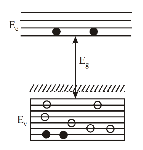
In the energy band diagram of a material shown below, the open circles and filled circles denote holes and electrons respectively. The material is
A
an insulator
B
a metal
C
an n-type semiconductor
D
a p-type semiconductor
Detailed Solution
The diagram shows an extra energy level lying in the energy gap $E_g$, slightly above the top $E_v$ of the valence band, with many holes (open circles) in the valence band.
Such a level is the acceptor energy level $E_A$, created by doping with a trivalent impurity (such as B, Al or In).
With a very small supply of energy an electron from the valence band can jump to the level $E_A$ and ionise the acceptor negatively.
Each such jump leaves behind a hole in the valence band, so holes become the majority carriers.
In an n-type semiconductor the extra (donor) level would lie just below the conduction band $E_c$, with electrons as majority carriers.
So the material is a p-type semiconductor.
Such a level is the acceptor energy level $E_A$, created by doping with a trivalent impurity (such as B, Al or In).
With a very small supply of energy an electron from the valence band can jump to the level $E_A$ and ionise the acceptor negatively.
Each such jump leaves behind a hole in the valence band, so holes become the majority carriers.
In an n-type semiconductor the extra (donor) level would lie just below the conduction band $E_c$, with electrons as majority carriers.
So the material is a p-type semiconductor.