Looking for classes? Ksquare Career Institute, Bengaluru →

Semiconductor Electronics: Materials, Devices and Simple Circuits
Formation of p-n Junction
2 questions from 2 papers, each with its answer.
- questions
- 2
- papers
- 2
- of Semiconductor Electronics: Materials, Devices and Simple Circuits
- 1.89%
Appears in
Concepts tested
- Direction of barrier potential
- Factors affecting barrier potential
All Questions
2003 AIPMT 1 question
-
Barrier potential of a p-n junction diode does not depend on -The barrier potential is set up by the immobile ions in the depletion region, formed by diffusion of carriers across the junction.
It depends on the semiconductor material (Si about 0.7 V, Ge about 0.3 V), the doping density (more doping gives a higher barrier) and the temperature (it decreases about 2 mV per degree rise).
It is changed by the applied bias: forward bias lowers the effective barrier and reverse bias raises it.
It does not depend on the design of the diode, i.e. its geometrical shape or construction.
So the barrier potential does not depend on diode design.
2002 AIPMT 1 question
-
In a PN junction : -When the junction forms, holes diffuse from the p-side to the n-side and electrons from the n-side to the p-side.
This leaves positively charged immobile donor ions on the n-side and negatively charged acceptor ions on the p-side of the junction (the depletion layer).
The positive charge on the n-side and negative charge on the p-side create an electric field from n to p. So the n-side is at a higher potential than the p-side; this is the barrier potential.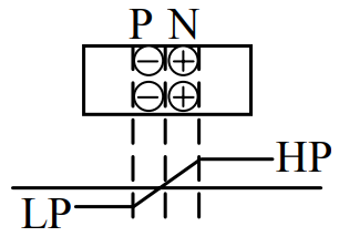
So there is high potential at the N side and low potential at the P side.