Looking for classes? Ksquare Career Institute, Bengaluru →

Semiconductor Electronics: Materials, Devices and Simple Circuits
Logic Gates
22 questions from 22 papers, each with its answer.
- questions
- 22
- papers
- 22
- years asked, 2017–2026
- 5 of 10
- of Semiconductor Electronics: Materials, Devices and Simple Circuits
- 20.75%
Appears in
Concepts tested
- Gate symbols 2
- Logic gates 2
- NAND truth table 2
- Truth table from waveforms 2
- truth table of a combination of gates 2
- AND truth table
- Combination of gates
- Combination of logic gates
- identifying a gate from a switch-LED circuit
- Identifying a gate from waveforms
- NAND followed by NOT
- NAND of inverted inputs equals OR
- NOR gate followed by a NOT gate
- NOR of inverted inputs
- OR gate followed by AND gate
- OR gate truth table
- output waveform of a logic circuit
All Questions
2023 1 question
-
For the following logic circuit, the truth table is:
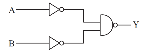
Circuit gives $y=\overline{\overline{A}\cdot\overline{B}}=A+B$ (OR), matching option (c).
$y=\overline{\overline{A}\cdot\overline{B}}$ $=A+B$ Truth table: A B Y 0 0 0 0 1 1 1 0 1 1 1 1
2022 1 question
-
The truth table for the given logic circuit is :
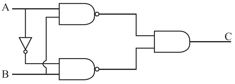 Outputs of the NAND gates: $\overline{A \cdot B}$ and $\overline{\bar{A} \cdot B}$ $C = \overline{A \cdot B} \cdot \overline{\bar{A} \cdot B} = \overline{A \cdot B + \bar{A} \cdot B}$ (De Morgan's theorem) $C = \overline{B(A + \bar{A})} = \bar{B}$ Truth table: (0,0) → 1, (0,1) → 0, (1,0) → 1, (1,1) → 0
2022 Phase 2 1 question
-
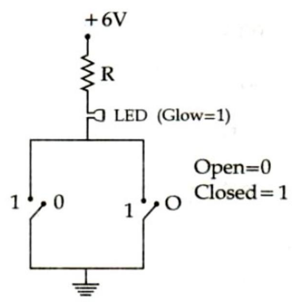 Identify the equivalent logic gate represented by the given circuit:When both switches are open (0, 0), no current flows and the LED does not glow (output 0). For inputs (0, 1), (1, 0) and (1, 1) at least one parallel path is closed, current flows and the LED glows (output 1). This is the truth table of an OR gate.
2021 1 question
-
For the given circuit, the input digital signals are applied at the terminals A, B and C. What would be the output at the terminal y?
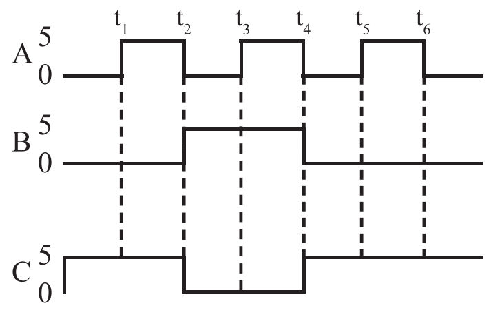
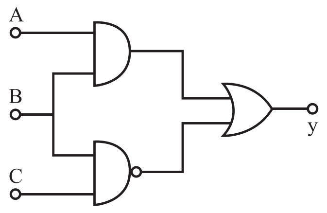 $Y = A \cdot B + \overline{B \cdot C}$
0 to $t_1$: A = 0, B = 0, C = 1 ⇒ $Y = 0 + \overline{0} = 1$
$t_1$ to $t_2$: A = 1, B = 0, C = 1 ⇒ $Y = 0 + \overline{0} = 1$
$t_2$ to $t_3$: A = 0, B = 1, C = 0 ⇒ $Y = 0 + \overline{0} = 1$
Checking all intervals in the same way, Y = 1 throughout, so the output is a constant 5 V (high).
2020 1 question
-
For the logic circuit shown, the truth table is:
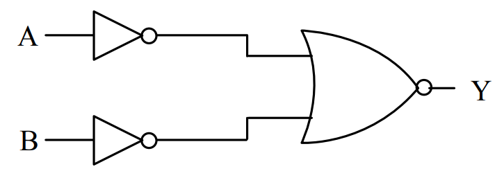 $Y = \overline{\bar{A} + \bar{B}} = \bar{\bar{A}} \cdot \bar{\bar{B}} = A \cdot B$ (AND gate)
Truth table: (0,0) → 0, (0,1) → 0, (1,0) → 0, (1,1) → 1
2019 1 question
-
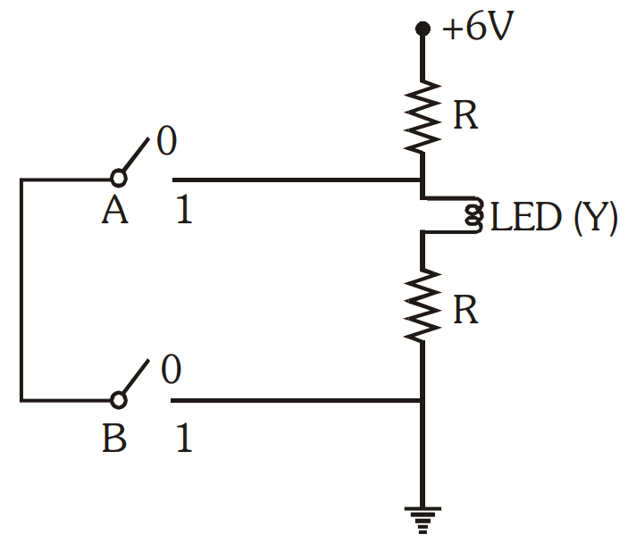 The correct Boolean operation represented by the circuit diagram drawn is:
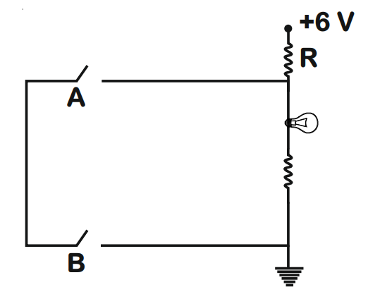
The LED glows when the voltage across it is high. From the circuit, the truth table is:
A = 0, B = 0 → Y = 1
A = 0, B = 1 → Y = 1
A = 1, B = 0 → Y = 1
A = 1, B = 1 → Y = 0
This is the output of a NAND gate.
2019 Odisha 1 question
-
The circuit diagram shown here corresponds to the logic gate,
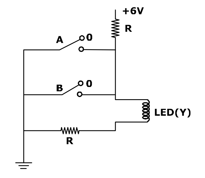 The switches A and B are in parallel across the LED path; closing either switch diverts the current away from the LED. The LED (Y) glows only when both A and B are open (0, 0), which is the truth table of a NOR gate.
2015 AIPMT-I 1 question
-
Which logic gate is represented by the following combination of logic gates? [add image]$Y_1 = \bar A$, $Y_2 = \bar B$, $Y = \overline{\bar A + \bar B} = A\cdot B$
Truth table (A, B → Y): 0,0 → 0; 0,1 → 0; 1,0 → 0; 1,1 → 1
This is the truth table of an AND gate.
2013 NEET 1 question
-
The output (X) of the logic circuit shown in figure will be:
 The first NAND gate gives $\overline{A\cdot B}$; the second NAND gate with joined inputs acts as a NOT gate.
$X = \overline{\overline{A\cdot B}} = A\cdot B$
2012 AIPMT-MAINS 1 question
-
To get an output Y = 1 in the given circuit which of the following inputs will be correct:
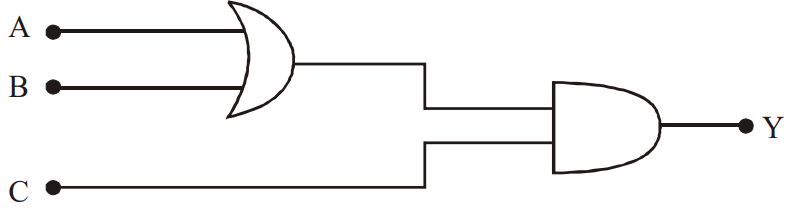 A and B feed an OR gate; its output and C feed an AND gate: $Y = (A + B)\cdot C$
For Y = 1 we need C = 1 and at least one of A, B equal to 1.
Only A = 1, B = 0, C = 1 satisfies this: $Y = (1 + 0)\cdot1 = 1$
2012 AIPMT-PRE 1 question
-
The figure shows a logic circuit with two inputs A and B and the output C. The voltage wave forms across A, B and C are as given. The logic circuit gate is
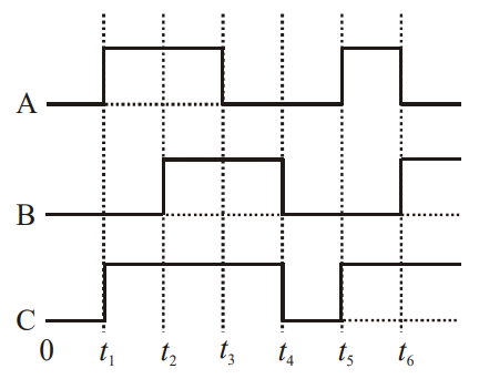 Reading the waveforms gives the truth table (A, B → C): 0, 0 → 0; 1, 0 → 1; 0, 1 → 1; 1, 1 → 1
The output is 1 whenever at least one input is 1, which is the truth table of an OR gate.
2011 AIPMT-PRE 1 question
-
Symbolic representation of four logic gates are shown as
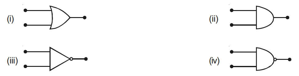
Pick out which ones are for AND, NAND and NOT gates, respectively.In the figure, (i) is the OR gate symbol (curved input side, pointed output).
(ii) is the AND gate symbol (flat input side and a semicircular, D-shaped output side with no bubble).
(iii) is the NOT gate symbol (a triangle with a small bubble at the output and a single input).
(iv) is the NAND gate symbol (the AND symbol followed by a small bubble at the output).
So AND, NAND and NOT gates are (ii), (iv) and (iii) respectively.
2010 AIPMT-MAINS 1 question
-
The following figure shows a logic gate circuit with two inputs A and B and the output Y. The voltage waveforms of A, B and Y are as given.
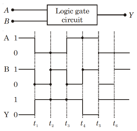
The logic gate isRead the input and output levels in each time interval of the waveforms and form the truth table.
A = 1, B = 1 gives Y = 0
A = 0, B = 0 gives Y = 1
A = 0, B = 1 gives Y = 1
A = 1, B = 0 gives Y = 1
The output is 0 only when both inputs are 1, and 1 otherwise. This is the truth table of $Y = \overline{A\cdot B}$.
Hence the gate is a NAND gate.
2010 AIPMT-PRE 1 question
-
To get an output Y = 1 from the circuit shown below, the input must be
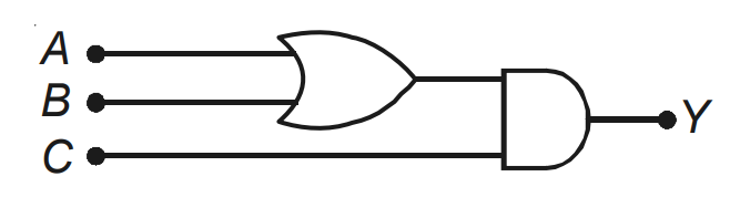 In the circuit, inputs A and B go to an OR gate, and the output of this OR gate together with C goes to an AND gate.
Boolean expression: $Y = (A + B)\cdot C$
For an AND gate the output is 1 only when both of its inputs are 1, so we need $A + B = 1$ and $C = 1$.
A = 1, B = 0, C = 0: $Y = (1 + 0)\cdot0 = 0$
A = 0, B = 1, C = 0: $Y = (0 + 1)\cdot0 = 0$
A = 0, B = 0, C = 1: $Y = (0 + 0)\cdot1 = 0$
A = 1, B = 0, C = 1: $Y = (1 + 0)\cdot1 = 1$
Hence the input must be A = 1, B = 0, C = 1.
2009 AIPMT 1 question
-
The symbolic representation of four logic gates are given below:
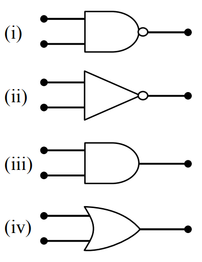
The logic symbols for OR, NOT and NAND gates are respectivelyIn the figure, (i) is the AND-shaped symbol (flat input side, rounded output) with a small bubble at the output: NAND gate.
(ii) is a triangle with a single input and a bubble at the output: NOT gate.
(iii) is the AND-shaped symbol without a bubble: AND gate.
(iv) has a curved input side and a pointed output, without a bubble: OR gate.
So OR, NOT and NAND gates are (iv), (ii) and (i) respectively.
2008 AIPMT 1 question
-
The circuit shown (a NOR gate followed by a NAND gate with both its inputs joined together, followed by a NOT gate) is equivalent to -
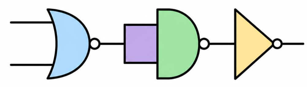 Let the two inputs be $A$ and $B$.
Output of the first (NOR) gate: $Y_1 = \overline{A + B}$
This output is fed to both inputs of the NAND gate. A NAND gate with its inputs joined works as a NOT gate:
$Y_2 = \overline{Y_1 \cdot Y_1} = \overline{Y_1} = \overline{\overline{A + B}} = A + B$
The last gate is a NOT gate, so the final output is $Y = \overline{Y_2} = \overline{A + B}$
$Y = \overline{A + B}$ is the output of a NOR gate.
Hence the combination acts as a NOR gate.
2007 AIPMT-PRE 1 question
-
In the following circuit, the output Y for all possible inputs A and B is expressed by the truth table
(A NOR gate with inputs A and B is followed by a second NOR gate whose two inputs are joined together.)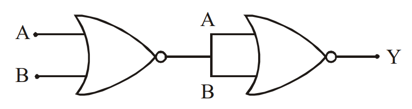
Each option lists the rows of the truth table as (A, B, Y).Output of the first NOR gate: $Y' = \overline{A + B}$
This output is fed to both inputs of the second NOR gate. A NOR gate with its two inputs joined acts as a NOT gate: $\overline{Y' + Y'} = \overline{Y'}$
$Y = \overline{Y'} = \overline{\overline{A + B}} = A + B$
So the combination works as an OR gate.
Truth table of $Y = A + B$:
A = 0, B = 0 gives Y = 0
A = 0, B = 1 gives Y = 1
A = 1, B = 0 gives Y = 1
A = 1, B = 1 gives Y = 1
So the truth table is (0, 0, 0), (0, 1, 1), (1, 0, 1), (1, 1, 1).
2006 AIPMT-PRE 1 question
-
The following figure shows a logic gate circuit with two inputs A and B and the output C. The voltage waveforms of A, B and C are as shown below -
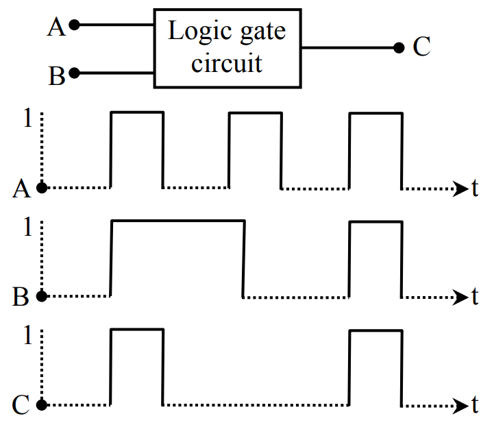
The logic circuit gate is :Read the waveforms interval by interval and compare the output C with the inputs A and B.
In the given waveforms the output C is high (1) only during those intervals in which both the inputs A and B are high (1).
Whenever either A or B (or both) is low (0), the output C is low (0).
This is the truth table of the AND gate: $C = A \cdot B$.
An OR gate would give a high output when any one input is high, and NAND and NOR gates would give a high output when both inputs are low.
So the logic circuit gate is an AND gate.
2004 AIPMT 1 question
-
The output of OR gate is 1 :-For an OR gate, $Y = A + B$.
Truth table: A = 0, B = 0 gives Y = 0; A = 0, B = 1 gives Y = 1; A = 1, B = 0 gives Y = 1; A = 1, B = 1 gives Y = 1.
So the output of an OR gate is 1 if either or both inputs are 1. It is 0 only when both inputs are 0.
(Output 1 only when both inputs are 1 describes an AND gate.)
2002 AIPMT 1 question
-
The given truth table is for which logic gate : -
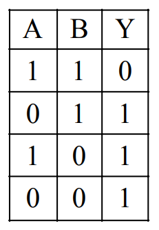 The output is 0 only when both inputs are 1, and 1 in all other cases.
This is the opposite (complement) of the AND gate output: $Y = \overline{A \cdot B}$
Check: AND gives 1, 0, 0, 0 for the four rows; its complement is 0, 1, 1, 1, which matches the table.
(XOR would give 0 for A = B = 0; NOR and OR do not match either.)
So the truth table is for the NAND gate.
2001 AIPMT 1 question
-
Following truth table represents which logic gate –
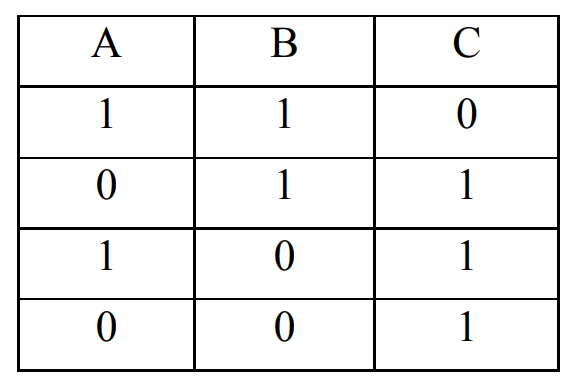 The output is 0 only when both inputs are 1; it is 1 for all other input combinations.
This is the complement of the AND output: $C = \overline{A \cdot B}$
AND would give 1, 0, 0, 0 for the four rows; its complement gives 0, 1, 1, 1, exactly as in the table.
XOR would give 0 for A = B = 0, and NOT has only one input.
So the truth table represents the NAND gate.
2000 AIPMT 1 question
-
Given truth table is correct for :
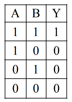 The output is 1 only when both inputs are 1; otherwise it is 0.
This is the AND operation: $Y = A \cdot B$.
So the truth table is for the AND gate.